A hardware team clears design review. Files go to the contract manufacturer. Then the first-article report comes back: tombstoned 0402 resistors, solder bridges across every fine-pitch QFN on the board, and a panelization layout that inflated unit fabrication cost by 20%. None of those problems showed up in the schematic. None of them were caught by the DRC. All of them were preventable.
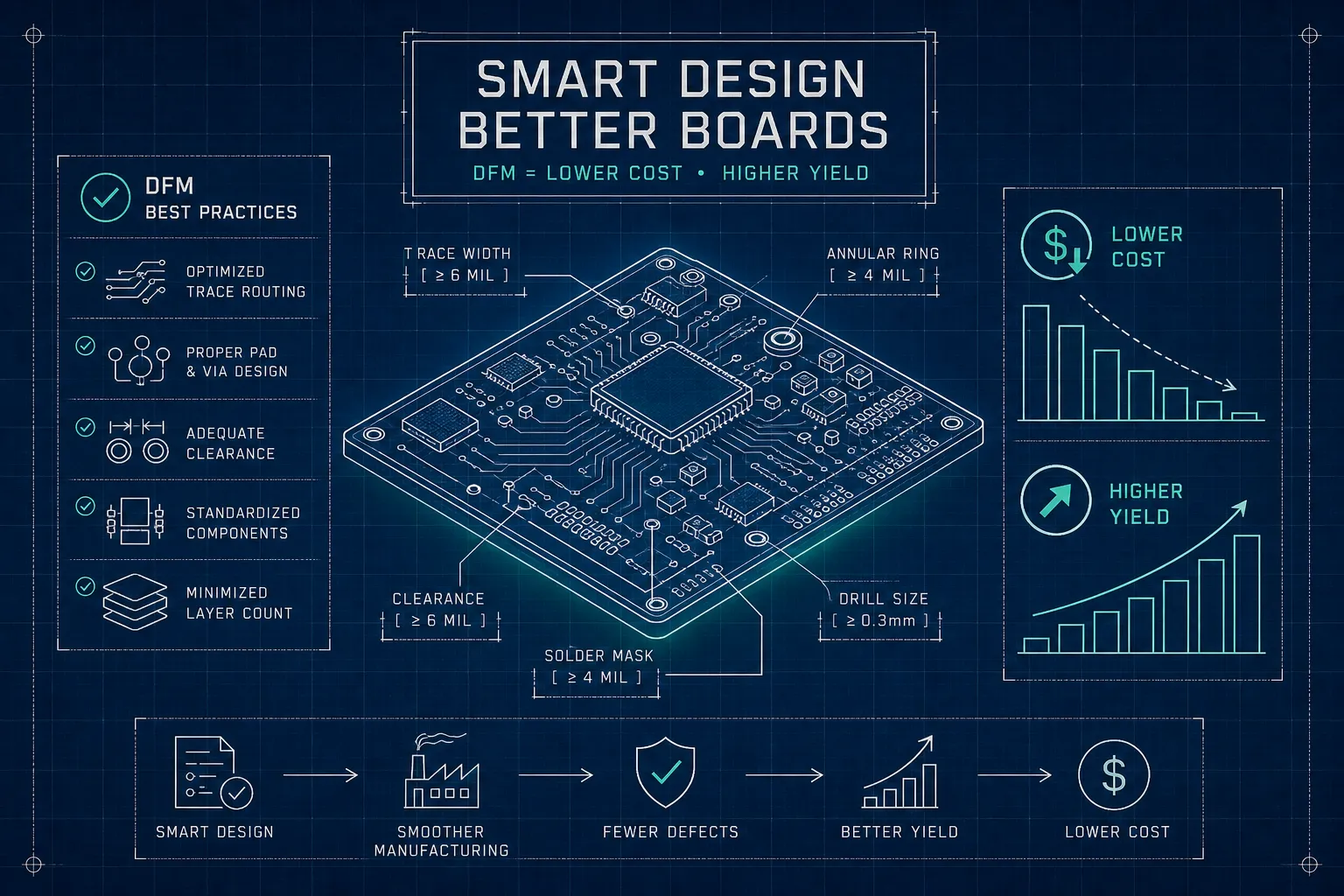
That gap between a “finished” PCB design and a manufacturable one is exactly what DFM principles are built to close. Design for manufacturability isn’t a single checkbox at the end of the layout process. It’s a collection of upstream decisions about pad geometry, via strategy, board outline, and component selection that directly determine yield, cost, and how smoothly your first build actually goes.
Contract manufacturers that conduct structured DFM reviews as part of their production readiness process can surface these issues before a single board goes into the reflow oven. Industry experience consistently shows that structured pre-release reviews reduce first-article defects and rework costs. This guide covers the four areas that drive the most preventable failures and cost: SMT pad design, via and drill decisions, panelization, and BOM hygiene. It then walks through what a real DFM review looks like before release.
Why DFM Failures Still Happen on Well-Designed PCBs
A large share of PCB failures aren’t caused by electrical errors. They’re caused by designs that are electrically correct but mechanically or thermally problematic for the assembly process. Engineers optimize for function; assemblers optimize for process repeatability. DFM is the translation layer between those two worlds. It sits within the broader DFX (design for X) framework, which also includes design for testability, design for reliability, and design for assembly (DFA), but DFM is the foundation because it determines whether the board can be built consistently in the first place.
The cost of getting this wrong extends far beyond the board itself. Rework labor, scrapped assemblies, and delayed launch timelines add up fast, and the engineering hours spent diagnosing failures that trace back to the layout stage only compound the damage. Benchmark data shows that architectural DFM changes (fewer layers, larger vias, better panel utilization) can reduce fabrication costs by tens of percent. Moving from 4 layers to 2 layers, for instance, eliminates one lamination cycle and reduces drilling complexity in a way that can cut per-unit cost by roughly 25 to 40 percent depending on vendor and volume. Catching those decisions early is prevention. Catching them after first article is an expensive reaction.
Design for Manufacturability Best Practices for Electronics: SMT Pad Design and Footprint Rules
IPC-7351 land pattern compliance is the baseline for SMT pad design, and non-compliant footprints are one of the most common root causes of tombstoning and solder bridging in first-article builds. The mechanism is straightforward: when pad geometry is asymmetric, or when copper connectivity on one side of a passive component is heavier than the other, one pad heats and wets before its counterpart during reflow. That unequal surface tension lifts the part. It’s a design flaw, not an assembly flaw, and it shows up consistently on 0201 and 0402 resistors and capacitors where the imbalance forces are large relative to component mass.
Tombstoning Prevention
Preventing tombstoning starts with symmetric footprints: matched pad dimensions, equal trace widths and copper area connecting to both sides, and thermal relief spokes for pads connected to large copper pours. Without thermal relief, a plane-connected pad pulls heat away faster than the isolated side, creating the wetting delay that causes the lift. IPC-7351 defines three density levels, maximum density for tight boards, median for most production contexts, and minimum for boards with relaxed spacing requirements. Matching the density level to your actual assembly environment is one of the more consequential footprint decisions you’ll make, since it directly sets pad extensions and courtyard boundaries for the entire board.
Solder Mask Dams and Fine-Pitch Parts
Solder bridging on fine-pitch parts like QFNs and BGAs is a function of paste aperture sizing, mask dam width, and mask registration. Targeting a 4 to 5 mil solder mask dam between adjacent pads is the practical minimum for most fine-pitch work; below that, mask-to-copper registration tolerances can eliminate the dam entirely, leaving no barrier between pads during reflow. These decisions belong in the PCB layout stage, not the first-article investigation report.
Placement Orientation and Keep-Out Zones
Component placement adds another layer of complexity. Polarity markings, pin-1 indicators, and component orientation relative to the reflow direction all affect assembly consistency. Crowding components or skipping orientation conventions creates manual rework risk that scales with volume. Keep-out zones around connectors and minimum spacing for automated pick-and-place should be locked in during placement, not treated as suggestions to be resolved at the CM.
Design for Manufacturability Best Practices: Via Strategy, Drill Sizing, and Stackup
Via geometry has a direct and often underestimated effect on fabrication cost. The practical standard tier for most contract manufacturers sits around 4 to 6 mil trace/space with a 0.15 mm finished hole and 0.15 mm annular ring. Advanced tier capabilities push to 2 to 3 mil trace/space, sub-0.15 mm holes, and HDI features like blind/buried vias and stacked microvias. The cost difference between tiers is significant, and the yield risk in advanced territory is real because tighter features require more process control to hit consistently.
One practical benchmark worth understanding: a 0.015-inch via versus a 0.010-inch via can double drilling throughput in some fabrication shops. That throughput difference translates directly into fabrication cost and lead time. Use advanced via geometry only when the design genuinely requires it. Via-in-pad, blind/buried vias, and stacked microvias all trigger advanced-tier pricing and should be justified by routing density or electrical constraints, not convenience.
For designs that do require via-in-pad, VIPPO (via-in-pad plated over) is the accepted method for any pad that will be soldered. An open via under a BGA pad is a reliability failure waiting to happen: solder wicks into the hole during reflow, creating voids and weak joints. VIPPO fills, planarizes, and plates over the via to create a flat solderable surface. It adds fabrication cost, but it’s the recommended approach for reliable via-in-pad under SMT components. Coordinate VIPPO requirements with your CM before layout is complete. The quality of the fill and cap plating varies by manufacturer and must be confirmed before you commit the design.
Test point access is a DFM consideration that gets skipped in too many reviews. Vias are natural ICT test points, but only if they’re accessible, consistently sized, and documented in the test plan. Burying test access under components or in via-in-pad configurations blocks flying-probe and ICT coverage, which means failures that could have been caught at test get shipped to the customer instead.
Panelization and Board Outline Planning: The Cost Lever Designers Overlook
Board outline decisions made in CAD directly determine how many boards fit per panel, which is the single biggest driver of per-unit fabrication cost after layer count. The relationship is proportional: a board shape that wastes a significant portion of a standard working panel raises unit fabrication cost by a roughly equivalent margin before any assembly runs. An outline that tiles efficiently on a standard panel size is a cost reduction built into the design itself.
Design for rectangular outlines where the product allows, plan for standard panel sizes, and discuss utilization targets with the CM before the board outline is finalized. Changing the board shape after layout is complete is expensive; changing it before placement begins costs almost nothing. In cases where a non-rectangular outline is required, nesting software or CM-led panel optimization can recover meaningful utilization that manual tiling misses, often delivering double-digit improvements in boards-per-panel.
V-scoring and tab routing are the two primary depanelization methods, and choosing correctly matters for both cost and component reliability. V-scoring is faster and cheaper, and it allows tighter spacing between boards, which improves utilization. However, the V-cut stress during depanelization can crack solder joints or damage components placed too close to the board edge. As a general rule-of-thumb followed by many CMs, keeping components at least 0.125 inches clear of board edges on V-scored panels reduces that risk, verify the exact clearance requirement against your CM’s process guidelines. Tab routing with breakaway tabs handles irregularly shaped boards more safely and limits depanelization stress, but the routing lanes consume more panel area.
Fiducial placement, tooling holes, and rail design should be in the layout from the start, not added by the CM as an afterthought. CNC routing tolerances run around ±0.2 mm; V-scoring tolerances are closer to ±0.5 mm. Building those tolerances into your component keep-out zones before the layout is complete is the right sequence. Leaving panelization entirely to the CM means giving up control over a cost variable that should be part of your design intent.
BOM Standardization and Component Lifecycle Hygiene as First-Line DFM
The BOM is a manufacturing input, not just a parts list. Components specified without alternates, in unsupported packages, or sourced from a single manufacturer create assembly risk before the first purchase order is placed. Choosing components that are available in the right package for your CM’s assembly process, carry healthy lifecycle status, and have at least one qualified alternate isn’t procurement hygiene. It’s DFM that starts at the component selection stage and feeds directly into your PCB manufacturability checklist.
An approved vendor list (AVL) locks in functionally equivalent alternates so the CM can build without a shortage-driven design spin. At Amtech, that AVL discipline connects directly to the Design for Volatility program: structured AVL development reduces both tariff exposure and supply chain disruption risk by ensuring every critical component has a validated second source before production begins. A BOM with no alternates is a single-point failure embedded in the design file, and it will surface at the worst possible time.
The most common BOM red flags that block DFM review sign-off are missing manufacturer part numbers, unresolved lifecycle conflicts, package mismatches where the schematic calls out a part that doesn’t match the footprint, and components available from only one distributor at an acceptable lead time. These aren’t difficult to fix early. They’re very expensive to fix after the first build is already scheduled.
What a Structured DFM Review Actually Looks Like
Automated DFM tools, including DRC, ERC, and fab rules checks, are first-pass screening. They catch rule violations, but they don’t catch engineering judgment errors like asymmetric thermal loading, poor test access, or a BOM full of single-source parts. A structured DFM review conducted by the CM’s engineering team covers the full release package: Gerbers or ODB++, fab notes, BOM with MPNs and alternates, pick-and-place centroid data, assembly drawings with polarity and orientation notes, stackup documentation, and the test point map. All of these need to be internally consistent for the review to pass.
Amtech’s production readiness reviews cover footprint compliance, thermal balance across the board, panelization optimization, BOM lifecycle status, and test point coverage. The corrections that come out of those reviews are specific and actionable: a pad geometry correction on a 0402 footprint contributing to tombstoning, a via-in-pad flag that would have shorted a BGA net, a panel layout revision that meaningfully increased boards per run. That’s what a real CM partnership looks like compared to a vendor that accepts files and builds whatever comes in.
The minimum complete package before a responsible release to fabrication includes:
- Schematic with ERC clean pass
- Gerbers or ODB++ with verified drill files and NC routing data
- Fab notes covering stackup, materials, finishes, controlled impedance, and tolerances
- BOM with MPNs, quantities, alternates, and lifecycle status
- Pick-and-place centroid file
- Assembly drawing with polarity, pin-1 indicators, and orientation notes
- Test point map with ICT or flying-probe coverage
- Mechanical outline and 3D model
Missing any of these doesn’t just delay the build. It creates assumptions the CM has to fill in, and assumptions in manufacturing become defects on the first article.
DFM Is a Design Discipline, Not a Final Gate
PCB manufacturability isn’t a review that happens at the end of the layout process. It’s a set of decisions embedded throughout layout, component selection, and documentation. Hardware engineers who internalize SMT pad rules, via constraints, panelization economics, and BOM hygiene catch problems in CAD that would otherwise surface as first-article failures. Applied consistently, these design for manufacturability best practices pay for themselves many times over in reduced rework, shorter build cycles, and better yield from the first run.
The best DFM outcomes come from treating the contract manufacturer as an engineering partner from the start, not a production vendor you hand files to after the design is locked. Bringing the CM in during layout, running a structured pre-release review, and building a complete documentation package before anything goes to fabrication is the standard that serious hardware teams work to.
Hardware teams approaching a new build or transferring a design to contract manufacturing should schedule a structured DFM review before release, not after first article. Amtech’s engineering team offers production readiness reviews built to surface exactly these issues before they cost you a production run. Connect with Amtech to schedule a DFM review or request a PCB manufacturability checklist to apply on your next design.