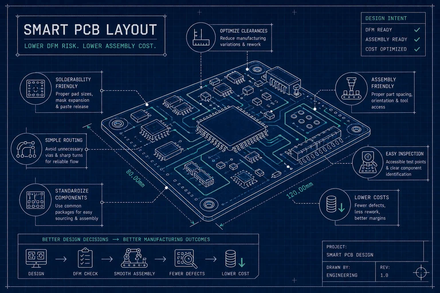
Most PCB cost overruns are locked in before the board ever reaches a contract manufacturer, a pattern that DFM research has documented across product categories for decades. Engineers concentrate on signal integrity and electrical correctness, hand off the design, and assume manufacturing cost is someone else’s problem. It isn’t. The layout stage is where the biggest cost decisions get made, and by the time a design reaches the fab, those decisions are already fixed. A layout-focused DFM cost reduction PCB layout review catches the largest cost drivers at the one point where they can still be changed without a full redesign.
This article covers the specific layout choices that translate directly into lower fabrication and assembly bills: layer count, via strategy, component orientation, trace routing, panelization, and surface finish. The sections below are ordered by cost impact, starting with the changes that move the needle most. At Amtech, our engineering team reviews layouts for exactly these issues before a single board is built, because that is where savings are real and actionable.
1. Layer count: the single biggest cost lever in your stackup
Layer count is the one design variable that produces the sharpest price jumps in PCB fabrication. Each additional layer adds lamination cycles, alignment steps, additional drilling passes, and more inspection surface area. The pricing impact is not subtle.
Moving from a 2-layer to a 4-layer board typically adds 35 to 40 percent to fabrication cost, a range consistently reported across fabricator quoting tools and industry DFM pricing guides. A 6-layer board can run close to twice the price of a comparable 2-layer design at low-to-medium volume. At high volume the per-unit effect softens, but the relative premium persists. Any layout review should start here: is every layer genuinely earning its place?
The goal is not to force a complex design onto fewer layers than it needs. It is to avoid adding layers for convenience. Common culprits include power planes added to simplify routing that could instead use wider traces, redundant ground pours on inner layers, and signal layers that exist because the designer ran out of routing room rather than because the stackup demanded it. Tighter routing discipline and better component placement can sometimes recover an entire layer, depending on routing density and overall placement efficiency.
There are real cases where adding a layer is the right economic call. A cleaner stackup with dedicated power and ground planes can reduce EMI-related rework, simplify test, and improve first-pass yield in ways that pay back the added fabrication cost. The decision should be made with actual cost data, not intuition. When Amtech reviews a layout, comparing routing complexity against layer count is always the first check.
2. Via choices that quietly inflate your fabrication bill
Via type is the most underestimated cost driver in PCB layout. Standard plated-through-hole vias are inexpensive to fabricate. The moment a design introduces blind vias, buried vias, laser-drilled microvias, or via-in-pad structures, the fabrication process changes class entirely.
Blind and buried vias can add 50 percent or more to fabrication cost compared to an equivalent design using standard PTH vias, depending on stackup complexity and via count. Via-in-pad adds plating, fill, and planarization steps that raise unit cost by 10 to 30 percent on their own. These premiums are consistent with HDI fabrication pricing data published by leading PCB fabricators. Many HDI designs require these structures for good reason, but designs that use them out of routing convenience rather than necessity are paying a significant premium they didn’t need to. For more on the specific cost implications of via-in-pad, see this analysis of the impact of via-in-pad on PCB manufacturing costs.
Via-in-pad is the right call for very fine-pitch BGAs and components where escape routing genuinely has no other path. Outside of those cases, the layout question to ask is whether the component could be placed or oriented to make via-in-pad unnecessary before committing to the structure. That single review step can eliminate one of the more expensive line items in a fab quote.
Via count itself matters less than via type, but excessive stitching vias, redundant test-point vias, and multi-via escape strategies all add drill time and inspection surface area. A routing pass specifically aimed at via reduction, consolidating returns, shortening trace runs, and using PTH alternatives where they exist, is one of the lower-effort layout changes with measurable fabrication cost impact. This kind of via optimization is a core part of PCB DFM best practices at the layout stage.
3. Component orientation and placement for lower assembly labor
Fabrication cost gets the most attention in DFM discussions, but assembly labor is where component placement and orientation decisions show up on the invoice. A layout optimized for routing convenience rather than assembly flow adds time at the pick-and-place machine, at the reflow oven, and at inspection.
Polarized components, electrolytic capacitors, diodes, and ICs, should be oriented consistently across the board so that all components of a given type share the same polarity direction. Random orientation means more opportunities for placement errors, slower visual inspection, and higher rework risk. Beyond polarity, limiting rotations to 0, 90, 180, and 270 degrees simplifies pick-and-place programming and reduces the chance of a technician verifying the same part twice under different orientations.
Components should also be placed so the board can complete assembly in a single reflow pass wherever possible. A second reflow pass adds cost, adds thermal stress to already-placed parts, and increases the chance of solder defects. Mixing fine-pitch SMD components with large through-hole or mixed-technology parts on the same board side forces the assembler to break the process into separate passes. Grouping components by package type and technology on the same board side reduces handling time and allows the line to run with fewer changeovers. Single-pass reflow is one of the clearest assembly cost targets a layout engineer can aim for directly.
4. Trace routing, board outline, and panelization for DFM cost reduction in PCB layout
Three layout factors directly control per-board fabrication price: trace-and-space tolerances, board outline geometry, and how well the design panels. Engineers control all three at the layout stage, and all three are easy to get right early and expensive to fix late.
At standard FR-4 with 1 to 2 oz copper, most fabricators treat 6/6 mil trace/space as the comfortable standard process floor, a threshold documented in the DFM guidelines published by major fab houses. Moving to 4/4 mil is achievable at capable fabs, but it often moves the order into a higher process class with a corresponding price premium. The same principle applies to via drill sizes: 0.30 to 0.40 mm drills hit the standard PTH floor for most fabs, while anything below 0.25 mm begins to trigger upcharges. For more detail on common manufacturing tolerances and their cost implications, see this overview of standard PCB tolerances. The cost impact is not from the geometry itself but from the process capability required to hold it reliably. Designing to standard tolerances is not conservative engineering, it is cost-conscious engineering.
Board outline shape determines how well boards nest on a manufacturing panel. Rectangular boards with no internal cutouts achieve the highest panel utilization, spreading fixed panel costs across the maximum number of units. Non-rectangular shapes, notches, and irregular geometry reduce that yield directly. For rectangular boards, V-score separation is cheaper to process than tab routing: it consumes less panel area, requires less machine time, and leaves cleaner edges. Tab routing is the right choice for irregular shapes, but for designs where the function permits a clean rectangular outline, preserving that outline keeps the separation method simple and cost-effective.
Panel rails, fiducials, and component clearance from the score line all affect how well a panel runs in production. Keeping components roughly 3 to 5 mm from V-score lines and copper clear of score paths prevents damage during depanelization. Both practices are worth confirming with your contract manufacturer before the outline is finalized; working through PCB panelization guide considerations at that stage is one of the faster ways to reduce per-unit price without touching the circuit.
5. Surface finish and laminate selection: matching spec to actual requirements
Over-specifying surface finish and laminate material is one of the quieter ways layout teams add cost to a design. Both choices should be driven by the application’s actual requirements, not by a default inherited from a prior design.
HASL and OSP are typically priced in the range of $0.05 to $0.08 per square inch of board area, based on widely published fabricator pricing. ENIG, with its additional gold layer and more complex process chemistry, runs roughly $0.12 to $0.25 per square inch. HASL is the practical choice for non-fine-pitch designs where solderability and reworkability matter more than surface planarity. OSP is the lowest-cost option for high-volume boards assembled quickly after fabrication, but its short shelf life and sensitivity to multiple heat cycles make it a poor fit for complex assemblies or boards with long storage windows. ENIG is justified for fine-pitch SMT components, BGA escape routing, and assemblies that require a long, reliable shelf life. Using ENIG on a design that would perform identically with HASL adds cost without adding value. For more on how different finishes affect assembly and cost, see this article on the role of surface finishes in PCB assembly.
Standard FR-4 is the correct laminate for the overwhelming majority of commercial and industrial designs. High-frequency RF designs, boards with tightly controlled impedance at GHz ranges, and assemblies operating in extreme thermal environments may genuinely require specialty laminates, but those are specific, engineering-driven exceptions. Defaulting to specialty laminates to add a margin of safety adds fabrication cost without a corresponding reliability benefit on standard applications. Every finish and material upgrade should be traceable to a functional requirement, not to habit.
Getting layout-level DFM review before your board goes to fab
The layout decisions covered in this article have the biggest cost impact when they are caught before the first production run. A DFM review at the layout stage prevents avoidable expenses from becoming fixed production costs. In many reported cases, DFMA practitioners and industry DFM programs have documented 25 to 50 percent cost reductions when these issues are addressed before tooling rather than after, though actual results depend on design complexity and how many cost drivers are present. For teams wanting a structured approach to reducing cost and lead time, reviewing DFM optimization strategies can be a practical next step.
A thorough layout-level review goes beyond running a standard DRC check. It examines layer count against routing complexity to identify consolidation opportunities, flags advanced via structures where PTH alternatives exist, evaluates component orientation for reflow efficiency, checks trace-and-space against the target fab’s actual process class, reviews board outline for panelization yield, and compares the specified finish to the assembly’s functional requirements. Each of those checks maps directly to a line item on a fabrication or assembly quote.
Amtech works with customers at the layout stage as part of its product development support process. Before a board goes to fabrication, Amtech’s engineering team reviews the design for the cost drivers described in this article and returns specific, actionable feedback. The goal is to reduce assembly labor and material cost in the revision before production begins, not to explain the overrun after it happens. For teams preparing a design for its first production run or working through a cost-reduction revision, that review is where the highest-leverage changes are identified.
The highest-impact changes are already in your layout
The biggest PCB cost reductions don’t come from squeezing your contract manufacturer on price. They come from layout decisions made before the board reaches the fab: fewer layers where routing allows it, standard PTH vias where advanced structures aren’t justified, component orientations that support single-pass reflow, trace tolerances that keep the design in a standard process class, rectangular outlines that maximize panel yield, and surface finishes matched to actual functional requirements.
Every one of those decisions is under the engineer’s control at the layout stage. Running a PCB layout DFM cost reduction review with your contract manufacturer before the first production order is the lowest-cost way to act on those decisions before they become fixed production costs. If your next revision is coming up, that review is the right place to start.
Reach out to Amtech’s engineering team to schedule a layout review before your next production run. For teams where DFM cost reduction in PCB layout hasn’t been part of the standard workflow, a single pre-production review is often where the most significant savings are found.