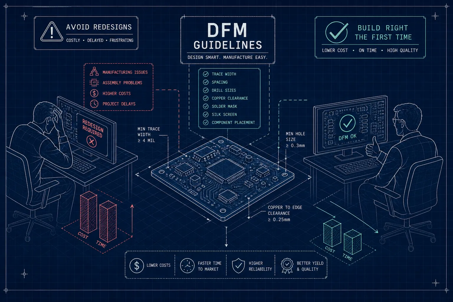
The fastest way to blow a schedule is a preventable board respin. Applying solid DFM guidelines early is what separates programs that hit first-article on the first attempt from those that spiral through expensive respins. Most redesigns trace back to issues a structured design for manufacturability review would have flagged early in the design phase. Fixing those issues on paper costs far less time and money. Fixing them after tooling, stencils, and first-article builds costs weeks and real money.
Your best leverage is early. The DFM guidelines below target the four places electronics programs most often stumble on manufacturability: PCB layout rules, component placement, tolerancing and pad geometry, and test access. Use them now, not after quote or kit release. At Amtech we embed DFM into onboarding for exactly this reason. Most problems are cheaper to catch before the first board exists than after it fails in the oven.
Apply these rules as you design, then run a process-specific checklist before file release. You will reduce rework, protect yield, and preserve headroom to scale.
Why most design problems survive until production
The cost multiplier nobody tracks
Change costs grow nonlinearly as you move from design to tooling to production. A clearance fix in your CAD file is free. The same fix after paste stencils and fixtures can be significantly more expensive once you factor in retooling, delays, and lost material, costs that multiply at each successive stage.
Consider a trace-to-copper clearance violation. Caught in Gerber review, you shift a trace by 4 mil (approximately 0.10 mm) and move on. Miss it, and you get random shorts, yield loss, and a surprise respin after first-article inspection. DFM done early converts expensive uncertainty into inexpensive edits.
How engineers unknowingly skip DFM
Many teams trust ERC and DRC in their CAD tool, then assume they are covered. Those checks validate electrical rules, not how a factory builds your board. DRC does not know your assembler’s nozzle clearances, stencil print limits, or ICT grid constraints. These are process-specific requirements that only a manufacturing-aware DFM review can catch.
The result is a design that passes every automated check yet fails manufacturability review. You only see it when a contract manufacturer refuses to quote without changes, or worse, when first-article data reveals defects you must now design around.
What a structured DFM review actually covers
DFM guidelines are not a single list. They are layered rules tied to each production step: PCB fabrication, SMT and through-hole assembly, test and inspection, and final box build. A complete review checks all layers together before file release.
For electronics, that means PCB DFM rules, DFA for placement and handling, DFT for probe access, and documentation alignment with standards like IPC-2221, IPC-7351, and IPC-6012. If your product includes enclosures, mechanical processes carry their own manufacturability rules, such as 2 degrees of draft for injection molding or generous internal radii for CNC pockets. The principle is consistent: design to the process window that will actually build your product. See our PCB Design Best Practices for practical checklists and examples.
PCB DFM guidelines that define what is buildable
The 4/4 mil safe default and when to push tighter
Rule 1: use 6 to 8 mil (0.15 to 0.20 mm) trace width and spacing as your default on standard FR-4. You will get better yield, more factory options, and fewer surprises. Many board houses will promise 4/4 mil, and it is achievable, but cost and risk both rise as you shrink the process window.
Rule 2: only drop to 4/4 mil, or to 3 mil in HDI or flex designs, with explicit fabricator agreement and a documented stackup. Advanced geometries pull you into premium fabrication classes and extra qualification. Tighter is not free, and it is never a default.
Drill, hole size, and annular ring margins
Rule 3: set the minimum finished hole size to 0.30 mm or larger when possible. Smaller drills are doable, but plating margin and yield improve as you step up in size. Many offshore lines will drill at 0.20 mm, yet boards become far less forgiving at volume. For further reading on how finished hole size impacts manufacturability, see minimum finished hole size and how it impacts manufacturability.
Rule 4: hold drill-to-copper clearance at 8 mil (0.20 mm) preferred, 6 mil (0.15 mm) minimum, and maintain at least 10 mil (0.25 mm) copper-to-board-edge. These clearances protect against drill wander, depaneling stress, and copper smear at the rails. Annular ring should leave real margin for production variation, not just pass your nominal CAD math. IPC-2221 provides the baseline and IPC-6012 governs acceptability; follow both and give yourself breathing room.
Stackup, aspect ratio, and via selection
Rule 5: keep via aspect ratio within 8:1 to 10:1. As the board gets thicker relative to the hole, plating coverage in the barrel center thins out, which hurts long-term reliability under thermal cycling. If you need denser routing, increase drill size, add layers, or engage your fab early on a controlled HDI stackup.
Blind and buried vias add cost, process steps, and risk. Use them only when placement density truly demands it, and call out any via-in-pad as filled and capped if it sits under a component. Reliability rises quickly when you design inside the plating window, not at the edge of it.
DFM guidelines for component placement that protect SMT assembly
Orientation, directionality, and reflow consistency
Rule 6: keep passives oriented consistently, and align the long axis perpendicular to the reflow conveyor where practical. Consistent orientation balances heating and reduces tombstoning forces, especially for 0402 and smaller parts. Center components on their pads and avoid asymmetric copper that heats unevenly across a joint.
Placement accuracy and thermal symmetry matter more than any single rule. A predictable reflow profile starts with predictable geometry.
Component-to-component and component-to-edge clearances
Rule 7: hold 0.25 mm body-to-body clearance as a practical minimum for standard SMT, and 0.50 mm or more around tall parts to preserve nozzle access and stencil contact. These are typical assembler guidelines; confirm with your specific CM, as requirements vary by equipment and process. Crowded footprints slow machines, complicate rework, and can trap paste at print.
Maintain edge clearance so parts do not collide with conveyor rails or depanel tooling. Connectors near the edge, tall electrolytics, and heat sinks all need extra margin to survive handling and depanelization without damage.
Keep-out zones and assembly-critical areas
Rule 8: define explicit keep-outs in the assembly drawing. Typical assembler guidelines recommend reserving approximately 1.25 to 2.00 mm around mounting holes for hardware and tooling, though the exact value depends on your hardware and fixturing. Protect connector mating envelopes, and mark regions that see flex or vibration in use. These are DFA requirements, not nice-to-haves. When you give your assembler clear keep-outs, you reduce quoting ambiguity and prevent late redesign requests.
Tolerancing, pad geometry, and via design that protect yield
Pad size, courtyard overlap, and solder bridging risk
Rule 9: use IPC-7351 land patterns and do not allow courtyard overlap. Undersized pads produce weak joints, and oversized pads on fine pitch invite bridges. Courtyards exist to represent real keep-out for placement and rework; if they overlap, your parts will fight each other in production. For practical pad sizing rules and examples, consult PCB pad size guidelines.
Footprint quality is one of the top causes of early assembly defects. Validate new or vendor-unknown parts with a footprint review, not a copy-paste from a random library.
When tight tolerances cross into specialty fabrication territory
Rule 10: if you need controlled impedance, controlled-depth backdrilling, or trace width tolerance tighter than your fabricator’s published standard capability, call it out explicitly in your fab notes and review it with the board house before committing. Boards built to “standard” tolerances will not magically meet RF or high-speed requirements by luck.
Use IPC-2152 for trace current sizing rather than legacy tables, specify controlled-impedance coupons, and attach the target stackup. If performance depends on the stack, document the stack.
Minimum feature size rules that affect stencil and paste deposit
Rule 11: keep solder paste aperture width at or above 0.20 mm, and preserve a stencil aperture aspect ratio above 1.5:1 for reliable release. Pair fine-pitch packages with an appropriate stencil thickness and aperture reduction strategy.
A great layout with a mismatched stencil still fails at print. Your DFM review should always connect component pitch to stencil spec and paste type before committing to tooling.
DFM guidelines for test access and DFT requirements your assembler will ask for
Test point size, spacing, and grid alignment
Rule 12: for ICT, target 1.0 mm diameter test pads on a 2.54 mm grid, accessible from one side. If space is tight, 0.89 mm pads on a 1.27 mm grid are possible at higher fixture cost and risk. Off-grid or hidden points push you toward flying probe, which is slower and expensive at volume.
Distribute test pads evenly, avoid placement under tall parts, and include a solid test reference point for ground. Good DFT looks boring, and that is the point.
Fiducial markers and panel registration
Place at least three global fiducials per panel near the corners, and add local fiducials at fine-pitch ICs. Keep a clear soldermask opening around each fiducial and avoid nearby copper that confuses vision systems.
Missing fiducials are a common reason an assembler pauses quoting to request a DFM update. Give the pick-and-place a trustworthy reference and placement accuracy follows.
How test strategy choice affects layout decisions
Choose the test strategy before layout freeze. If you plan ICT at production, prioritize probe access on the test side and include fixture keep-outs. If you will rely on functional test, still provide defined pads for rework and failure analysis so debug is not guesswork.
Retrofitting test access after routing is almost always a respin. Decide early and route to the decision.
What a DFM review with your CM should look like before first build
What to submit and what your CM is checking
Send complete data for review. That package should include:
- Gerbers or native CAD outputs
- A fabrication drawing with controlled-impedance notes where applicable
- Drill files
- The full BOM with approved vendors
- A coherent assembly drawing
A thorough DFM review checks trace and clearance rules, hole and annular ring geometry, component placement and courtyards, stencil and pad alignment, test access, fiducials, and the completeness of fab notes aligned to IPC-2221, IPC-7351, and IPC-6012. The goal is to surface and correct every issue before material orders, stencil cut, or fixture build. Identify every change on paper, not on the factory floor.
How Amtech embeds DFM into its onboarding process
At Amtech, every new program typically begins with a structured DFM and DFT review run by our manufacturing and test engineers. We work to reconcile your design intent with real process windows, flag risks such as tight aspect ratios, missing test points, or courtyard conflicts, and loop quickly with your team to close them before production begins. Read more about Why Design for Manufacturability (DFM) Can Save You Millions for an expanded discussion on the business impact of early DFM.
Our lines use AI-enabled inspection and robust traceability, which informs our understanding of which design patterns tend to cause production issues. That process knowledge is what we bring into early DFM reviews to help protect first-article yield and support a stable ramp with fewer unnecessary spins.
Using DFM output to build a reusable checklist
Treat each DFM finding as an input to a living checklist you apply at schematic freeze and again at pre-release. Teams that build this habit commonly report shrinking review cycles and faster quote turnarounds. Start with these process-specific checkpoints:
- Fabrication checklist: target 6 to 8 mil (0.15 to 0.20 mm) trace and space, confirm any 4/4 mil or HDI features with the board house, set finished hole size at 0.30 mm or larger where practical, hold 8 mil (0.20 mm) drill-to-copper and 10 mil (0.25 mm) copper-to-edge, lock stackup and via aspect ratio to 8:1 to 10:1 with notes tied to IPC-2221 and IPC-6012.
- SMT assembly checklist: validate footprints to IPC-7351, check for courtyard overlap, standardize passive orientation, enforce 0.25 mm body-to-body minimum and 0.50 mm near tall parts, review stencil thickness and fine-pitch apertures for aspect ratio above 1.5:1.
- Test and inspection checklist: place 1.0 mm pads on a 2.54 mm grid for ICT or document the flying-probe plan, add global and local fiducials with clear soldermask openings, define fixture keep-outs, and include test pads for debugging even when functional test is the primary strategy.
Conclusion
The most effective DFM guidelines live where mistakes are most common: PCB layout and trace rules, component placement for SMT, tolerancing and pad geometry, and test access. The value is not in owning a long checklist, it is in applying the right checks before files leave engineering. Adopt these design for manufacturability guidelines as part of your pre-release process to reduce redesigns and improve first-article yield. Fixing on paper is cheap. Fixing after stencils and fixtures is not.
Teams that make DFM review a consistent part of their pre-production workflow tend to see fewer redesigns, better first-article yields, and faster ramps to volume. If you want a manufacturing partner that runs this process alongside you, Amtech embeds structured DFM and DFT review into program onboarding, works through issues quickly, and hands your design to production already reconciled with real factory limits. Send us your design package and we will help you turn uncertainty into a buildable plan, learn more about our approach to DFM and program onboarding.