
A defect that costs around $1 to fix at the AOI inspection stage can run $100 or more by the time the same board reaches final test, and closer to $1,000 or beyond once it reaches the field, once you factor in logistics, warranty processing, and the reputational damage that follows a customer return. The gap between a first-pass yield of 95% and 99% isn’t a minor quality footnote. It’s the difference between a profitable production run and one buried in rework labor, replacement parts, and missed ship dates. That’s exactly why automated PCB inspection has become a non-negotiable part of any serious SMT assembly operation.
At Amtech, inline inspection is built into the production flow from the moment solder paste hits the board, not bolted onto the end of the line as an afterthought. This article breaks down how AOI, X-ray, and SPI work, what each one catches, how they compare, and what to look for when you’re evaluating or deploying a system.
Why catching defects early changes the economics of PCB assembly
The cost multiplier effect in PCB assembly is well-documented and genuinely punishing. Industry data places the cost of fixing a defect at the AOI stage at roughly $1. That same defect found at functional test runs about $100. Field returns push toward $1,000 or more when you account for logistics, warranty processing, and the reputational hit that follows a customer return. Rework at late stages typically runs 10x or more per stage relative to early-stage correction, roughly $1 at AOI, $100 at functional test, $1,000-plus in the field, and that math compounds fast when you’re building in volume.
The practical implication is that every defect escaping an earlier inspection checkpoint becomes significantly more expensive to resolve. Full board desoldering, component replacement, and re-inspection aren’t just time-consuming. They affect delivery schedules, burn technician hours, and on high-value boards with complex assemblies, they can push the economics of a production run into the red.
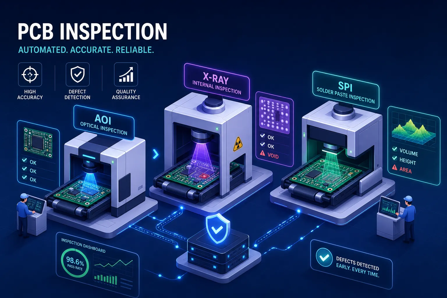
A typical SMT production line has three natural inspection checkpoints, each targeting a different defect class. SPI runs after the stencil printer and before component placement, checking paste deposition before anything else happens. AOI runs post-reflow, catching assembly placement errors and visible solder joint defects after the oven. X-ray and functional test handle complex packages and complete builds at the back end of the line. Missing any one of these checkpoints means defects that were cheap to fix get pushed into the next stage, where they’re expensive.
What automated optical inspection actually detects
AOI excels at surface-visible assembly defects, and the detection rates for these are consistently strong in production environments. Modern, well-programmed PCB visual inspection systems achieve 95 to 99.5% detection on common SMT defect categories. AI-assisted systems on mature production lines push that to 98 to 99% on critical solder joints, with under 1% false positives when properly calibrated and trained on real production data.
AOI for PCB: common defect categories
AOI reliably covers a broad range of surface assembly defects, including missing components, wrong polarity or orientation, misalignment and skew, solder bridges, tombstoning, insufficient or excess solder on visible joints, and surface contamination or scratches. These aren’t edge cases, they represent the majority of defects generated in a standard SMT assembly process, which is why machine-vision PCB inspection in the form of AOI is the workhorse method on most production lines.
3D AOI vs. 2D AOI
That said, AOI has hard limits, and you need to plan around them. Any solder joint hidden under a package is invisible to top-side optical imaging. BGAs, QFNs, CSPs, and other bottom-terminated components hide their joints completely. Micro-voids, internal cracks, and subsurface defects are equally invisible. Traditional 2D AOI detection rates for tiny lead-free micro-defects drop as low as 15 to 50% without advanced algorithms. True 3D AOI is the most impactful upgrade for boards with fine-pitch components, lifted leads, or IPC-A-610 height-based acceptance criteria, two-dimensional imaging simply can’t measure what isn’t visible from one flat plane. This isn’t a failure of AOI as a category. It’s a scope issue: automated PCB inspection via optical methods is a surface inspection discipline, and the moment a defect moves below the surface, you need a different method.
SPI and X-ray inspection: covering what AOI can’t see
Solder paste inspection sits at the very front of the SMT line, running after the stencil printer and before component placement. It measures paste volume, height, area, and alignment for every pad on the board. The reason this matters: roughly 60 to 70% of PCB assembly defects trace back to solder paste problems. Catching an off-spec deposit before reflow costs almost nothing to correct. Correcting the solder joint defect that results from that same deposit, after the board has run through the oven, is a different conversation entirely.
SPI also feeds real-time process feedback into the production loop. When paste deposits drift outside spec, the system flags the printer for adjustment before a systematic error propagates across a full panel. That feedback capability is what separates SPI from a simple pass/fail gate: it actively prevents defect classes from repeating, which is where the yield improvement actually accumulates.
Automated X-ray inspection (AXI) picks up where both AOI and SPI leave off. It’s the only non-destructive method capable of verifying solder joint quality under BGA, QFN, LGA, and similar packages. X-ray reveals voids, head-in-pillow defects, insufficient solder fill, bridging under the package, and internal structural issues that no surface inspection method can reach. For any board with bottom-terminated components or high-reliability requirements, medical, aerospace, automotive, or other safety-critical applications, X-ray isn’t optional. It’s the only way to confirm what optical inspection physically cannot see.
AOI vs. X-ray vs. ICT vs. functional test: matching the method to the fault
Each inspection method is optimized for a different fault profile, and none of them alone covers everything a production board can generate. AOI handles fast, high-throughput screening of visible assembly defects. AXI targets hidden solder joints and internal structural issues. ICT verifies electrical continuity, net connectivity, and component values when test access is available. Functional test confirms the board behaves correctly under real operating conditions but can miss latent assembly defects that don’t affect the specific test scenario being run.
Where the methods diverge is instructive. A solder bridge that’s visible at the board edge will be caught by AOI. The same type of bridging hidden under a BGA requires X-ray. A wrong-value component that AOI might miss because it’s the right package size will often be caught by ICT if the value affects a measurable net. A timing fault or interface failure that has nothing to do with assembly defects requires functional test to surface. The fault determines the method, not the other way around.
Configuration decisions should follow the same logic. A simple single-side board with no BGAs and low reliability requirements may need only AOI. A dense, BGA-populated board for a high-reliability application needs AOI plus AXI at minimum, likely paired with functional test. The practical rule: layer inspection methods based on the defect classes your specific assembly generates, not on what every method can theoretically do.
What to look for when evaluating an automated PCB inspection system
Camera resolution is the starting point for any serious evaluation of AOI for PCB work. For fine-pitch SMT work, target 10 to 15 µm per pixel. As pitch demands have tightened over the past decade, systems have moved from 0.3 MP to 20 MP-plus, and that progression reflects real production requirements rather than marketing specs. Higher resolution improves defect detectability on shrinking features but increases processing load, so throughput and resolution have to be balanced against your actual line speed.
Multi-angle RGB lighting matters more than most buyers initially realize. It separates solder, copper, and silkscreen in the image, reveals fillet geometry under oblique angles, and requires daily calibration because LED aging changes how solder joints appear over time. IPC-A-610’s visual acceptability criteria for fillet shape, solder volume, and wetting geometry require the kind of dimensional data that only 3D systems deliver consistently, a strong argument for 3D over 2D on any board with fine-pitch components or strict acceptance criteria.
On throughput, modern inline automated PCB inspection systems run 250 to 1,800 boards per hour depending on board complexity and resolution settings. False call rates below 100 ppm are achievable in well-tuned systems. Some ML-assisted deployments report 99.7% detection accuracy with 0.4% false positive rates, those numbers are achievable on mature, well-trained lines, so plan for a ramp period to reach them.
On cost, entry-level inline AOI typically runs $50,000 to $90,000 for equipment, with programming and calibration adding $10,000 to $30,000 and annual maintenance in the $500 to $2,500 range for simpler systems. High-end 3D AOI systems land in the $150,000 to $250,000 range, with annual maintenance often running 15 to 22% of list price. Premium turnkey integrated inspection lines can reach $1.2 million-plus. For most mid-size contract manufacturers, a $100,000 to $200,000 fully commissioned 3D inline system delivers the best performance-to-TCO ratio, with typical ROI payback of 12 to 18 months on stable production lines.
Deploying automated PCB inspection in a production line that actually works
Before committing to a system, the evaluation has to connect hardware specs to real production requirements. The right questions to ask are specific: What is the smallest defect size your boards require you to detect? Do you have BGA or QFN components that need X-ray coverage? What is your current false call rate, and how much operator time goes toward confirming false alarms? Does your line speed support the inspection throughput of the system you’re evaluating? Can the software handle fast program setup for high-mix production without recreating inspection definitions from scratch for every new board?
These questions matter because inspection systems are only as effective as the process they’re integrated into. A high-resolution 3D AOI system with poor program libraries and no process feedback loop produces false alarms, breeds operator fatigue, and eventually gets bypassed. Software quality, fiducial-based alignment, and rule reuse across similar board families are what separate a system that improves yield from one that creates noise.
At Amtech, automated PCB inspection runs inline at the paste, post-reflow, and final assembly stages as a matter of production practice. Each checkpoint feeds real-time data back into the process rather than operating as an isolated quality gate. That’s how inspection automation actually prevents defects from recurring rather than simply catching them after they’ve already been built. For high-reliability applications in industrial, aerospace, and IoT electronics, this kind of integrated inspection strategy is what separates assemblies that survive the field from ones that look fine at ship.
Building the right automated PCB inspection strategy for your boards
The question isn’t whether to invest in automated PCB inspection, it’s whether the inspection strategy in place is actually matched to the complexity and reliability requirements of the boards you’re building. That means selecting methods based on the defect classes your assemblies generate, layering them across the right checkpoints in the production flow, and maintaining the process discipline that turns inspection data into sustained yield improvement.
When you’re evaluating a manufacturing partner or building out your own line, ask whether their inspection coverage extends to paste deposition, post-reflow surface defects, and hidden solder joints under complex packages. If any of those checkpoints is missing or treated as optional, defects that were cheap to fix will keep finding their way to the stages where they’re expensive. If you’re not confident your current approach covers all three, that’s worth examining before the next production run.