The phrase “AI hardware” gets thrown around constantly, and almost never precisely. Product teams are making six-figure architecture decisions based on spec sheets they half-understand, and founders are nodding along in conversations about NPUs and tensor cores without a firm grasp of what actually matters for their specific workload. That’s a real problem, because the wrong chip choice doesn’t just waste money; it shapes deployment timelines, energy costs, and the entire product architecture downstream.
This guide cuts through that noise. You’ll learn what the main processor types actually do, why training and inference pull hardware in completely opposite directions, how to match your deployment model to the right platform, and what most product teams discover too late when they try to build AI systems at scale. At Amtech, we work directly with engineering teams bringing complex AI hardware products from design through production, and we see firsthand where technical decisions get made well and where they fall apart. The chip spec is usually not where things break.
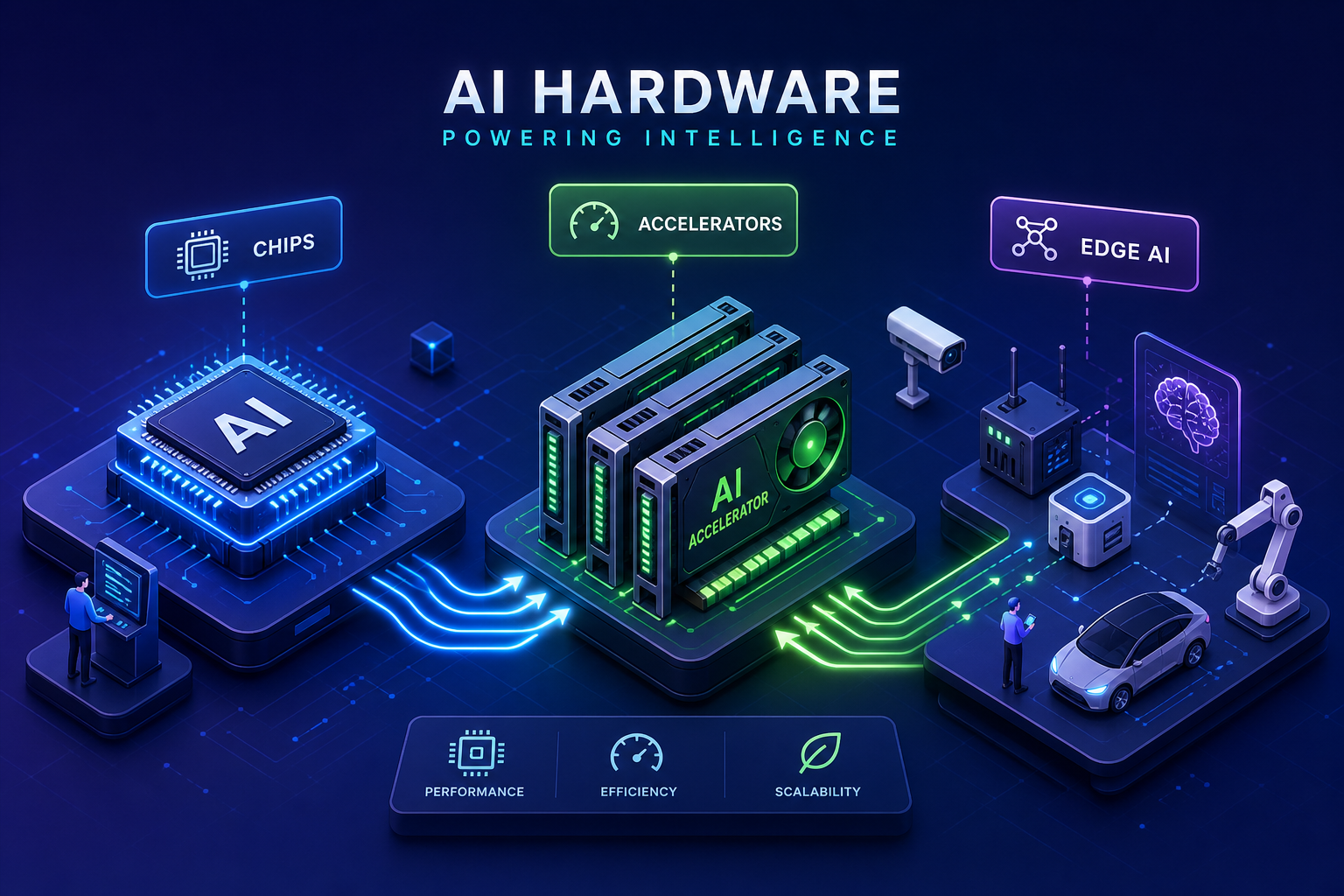
What makes AI hardware fundamentally different from standard computing
CPUs are genuinely excellent processors, but they’re built for a different class of problem. A CPU excels at sequential, control-heavy tasks: branching logic, orchestration, general computation, and operations that require rapid context switching between very different processes. That’s the wrong architecture for AI. A neural network doing inference is essentially running an enormous matrix multiplication loop millions of times per second, and a CPU was never designed for that kind of workload.
AI workloads are inherently parallel. Thousands of operations need to run simultaneously, not one after another. Matrix multiplications, dot products, and convolution operations all map cleanly onto hardware with thousands of small cores working in unison. This is the core reason AI accelerators emerged as their own category: the architectural shift from serial to parallel compute isn’t an incremental improvement; it’s a fundamentally different way of building silicon. Understanding that shift is the starting point for every hardware decision that follows.
The main AI chip types and what each one does best
GPUs are the workhorses of AI compute. Their massive parallelism, mature software ecosystems (CUDA, PyTorch), and broad framework support make them the default choice for both training and inference across most use cases. TPUs are Google’s purpose-built tensor accelerators, optimized specifically for large-scale deep learning within TensorFlow and Google Cloud environments. They’re highly efficient for supported workloads but carry real ecosystem lock-in. ASICs represent the far end of the efficiency spectrum, chips designed for one specific task that deliver peak performance-per-watt, but they require significant upfront investment and offer almost no flexibility once taped out.
NPUs occupy a different position entirely. Purpose-built for neural network inference, they’re commonly embedded in smartphones, edge devices, and industrial systems. The design priority is low power draw over raw throughput, which makes them well-suited for always-on applications with tight energy budgets. FPGAs offer a different trade-off: reconfigurable hardware that can be customized after manufacturing, making them valuable for prototyping AI accelerators, low-latency inference tasks, or workloads where no off-the-shelf chip fits cleanly.
The decision map simplifies once you know your workload:
- CPU: preprocessing, orchestration, and small models
- GPU: training and general-purpose inference
- TPU: large-scale training in Google-ecosystem environments
- NPU: on-device edge inference with low power budgets
- FPGA: custom low-latency workloads and prototyping
- ASIC: high-volume targeted applications where performance-per-watt is the primary metric
Training vs inference: why hardware requirements diverge completely
What training actually demands from your hardware
Training a model is computationally expensive in ways that inference is not. Every training iteration requires a forward pass, backpropagation, gradient calculation, and weight updates across every batch in the dataset. That demands enormous sustained FLOPS, high-bandwidth memory, and the ability to hold that compute load for hours or days without throttling. Memory capacity matters as much as raw compute here. A GPU that handles inference on a given model may not carry enough VRAM to train it. An NVIDIA A100 delivers around 19 TFLOPS at FP32; Blackwell-class chips push into hundreds of TFLOPS on tensor cores, with the NVIDIA H100 SXM running at a thermal design power above 700W and the B200 approaching 1000W. For a concise primer on the practical differences between these workloads, see this overview of the difference between AI training and inference.
Inference runs only a forward pass. Per-request compute requirements are significantly lower, and the hardware selection logic shifts accordingly. The relevant metrics for inference hardware are latency, throughput per dollar, and energy efficiency, not peak FLOPS. Smaller GPUs, NPUs, or dedicated inference accelerators frequently outperform flagship training GPUs on a performance-per-watt basis. Cloud inference benchmarks have shown NVIDIA hardware delivering over 100 server queries per watt on certain workloads, but the right efficiency metric depends entirely on your model architecture and serving requirements.
Edge inference and the constraints that change everything
Edge inference takes the optimization calculus further. When inference runs on a device in the field, power envelope, form factor, and thermal budget become the dominant design variables, not just compute and memory capacity. A chip that performs brilliantly in a data center may be completely unsuitable for a device running on battery power inside an industrial enclosure.
Cloud, on-prem, and edge: matching hardware to your deployment model
Cloud GPU instances give you access to high-end accelerators without capital expenditure. H100 instances run roughly $1 to $7 per GPU-hour on alternative cloud providers, and $7 to $12-plus per hour on major hyperscalers on-demand. If you need a quick comparison of pricing across providers, this GPU cloud pricing comparison is a useful starting point. Cloud wins when workloads are bursty, the team is early-stage, or training jobs run infrequently. The general threshold is around 30 to 40 percent sustained utilization; below that, cloud economics tend to be favorable over owned infrastructure.
On-prem makes sense when utilization is high and predictable, when data residency requirements are strict, or when the business needs multi-year cost predictability. For local LLM deployment, the hardware tier depends on model size. RTX 3090 or 4090 cards with 24GB VRAM handle models in the 13B to 34B parameter range well. Workstation-class A6000 or A100 cards support 70B-plus models with room to work. Apple Silicon with unified memory, particularly M3 Pro or Ultra configurations, offers a power-efficient option for smaller local workloads where GPU VRAM isn’t the primary bottleneck. Factor in power, cooling, and staffing costs. On-prem infrastructure rarely runs itself.
Edge AI inference runs near the data source: inside machines, on devices, or in the field. NVIDIA Jetson platforms and Google Coral TPU modules are the most common deployment targets. Model size is constrained to what quantized models in the 1.5B to 7B range can handle within the available thermal and power envelope. For edge AI systems, thermal budget, power draw, and physical form factor are not afterthoughts. They need to be addressed at the PCB design stage, before the product goes anywhere near production.
Why AI hardware is unusually complex to build and what product teams miss
The chip selection conversation is necessary, but it’s not where AI hardware projects typically run into trouble. The problems show up at the board level, in manufacturing, and in supply chain. Teams that treat these as downstream concerns almost always pay for that assumption in rework cycles and delayed launches.
Thermal management starts at the PCB, not in the enclosure. An H100 SXM has a thermal design power above 700W; the B200 pushes toward 1000W. At the board level, managing that heat means thermal via arrays, copper pours, deliberate component placement, and sometimes active cooling integration built directly into the board design. Edge AI hardware compounds the challenge: passive cooling is often the only option, which means thermal decisions made during layout directly constrain what the product can do in the field. Teams that treat thermal management as a post-design problem find themselves doing expensive board respins after prototypes start derating under load.
High-density PCBs for AI products combine high-speed DDR and HBM interfaces, dense BGA components, multi-layer controlled impedance routing, and mixed-signal sections running simultaneously. Getting the layout right requires engineers who understand both signal integrity requirements and manufacturing tolerances, and the two don’t always point in the same direction. HDI techniques like microvias, blind and buried vias, and via-in-pad structures are often necessary, but only up to the process capability of the fab you’re working with.
Supply chain adds another layer of complexity. Specialized AI chips, HBM memory modules, and power management ICs are currently running lead times in the 20 to 40 week range in some categories, with HBM and enterprise memory products frequently moving to allocation-only status. Missing that reality during BOM planning means schedule slippage that no amount of engineering excellence can recover. For a manufacturing-side perspective on these logistics and partnerships, listen to the AI in the Manufacturing Supply Chain: A Conversation with SnapChip, Amtech podcast.
This is where product teams building AI hardware for the first time typically hit a wall: strong chip selection, solid firmware, and a PCB layout that’s difficult to manufacture reliably at volume. Amtech’s engineering team works through DFM reviews, thermal design feedback, and component risk analysis before a single board goes into production, learn more about our approach in Inside Amtech’s Tech Stack: How We Built AI to Accelerate Scope of Work and Troubleshooting, Amtech. That front-end collaboration is what separates a clean product launch from a costly rework cycle. The technical complexity of AI hardware doesn’t pause once the design is done; it shifts into manufacturing, and a partner who understands both sides of that transition makes the difference.
Choosing the right hardware for your AI workload
AI hardware is a set of deliberate trade-offs between compute, memory, power, flexibility, and cost. There’s no universal answer, but the right answer for your workload becomes clear once you know what problem you’re actually solving.
Training at scale requires high FLOPS and large memory capacity sustained over long compute runs, GPU clusters or TPU pods in cloud or on-prem configurations. Low-latency cloud inference shifts the priority to throughput efficiency and cost per request. Edge inference reframes the entire equation around power envelope and form factor, with chip selection driven as much by thermal constraints as by model performance.
Revisiting the decision map from section two: use CPUs for preprocessing and small models, GPUs for general training and inference, TPUs for large-scale Google-ecosystem workloads, NPUs for on-device edge inference, FPGAs for custom or prototyping workloads, and ASICs for high-volume targeted applications where efficiency is the top priority. Most real-world deployments use more than one of these in combination, and the architecture decision is about knowing which chip carries which workload.
For teams taking an AI hardware product from design through to production, the technical complexity doesn’t stop at the chip spec. Thermal design, high-density PCB layout, and supply chain planning are engineering problems in their own right, and they require a manufacturing partner with the depth to address them from the start. If you’re moving from prototype to production and want a partner who works through those problems before they become expensive, Amtech is the right conversation to start. Tell us where your build is and we’ll tell you what it needs, and read more about AI in Electronics Manufacturing: What’s Really Changing, Amtech to see how these challenges look in real product workflows.