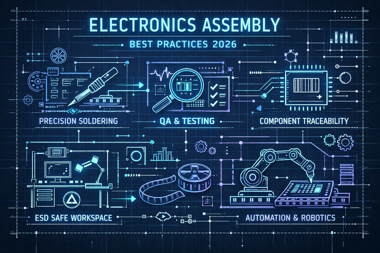
Electronics assembly decides whether a design clears qualification or ends up trapped in rework and cost overruns. A handful of focused checks early in development cuts scrap, speeds PCB assembly, and reduces time on the SMT line. These five practical best practices improve circuit board assembly and make downstream EMS handoffs more predictable.
What you need to know
For electronics assembly, start with early DFM and a hardened BOM so part choices and footprints don’t cause solder failures or supply shocks. Standardize inspection and process control to IPC-A-610 and J-STD-001, lock down reflow and placement profiles, and use SPI/AOI/AXI where appropriate. Match test strategy to volume and pick the production path: prototype, in-house, or EMS, based on NRE, testability, and expected demand.
1. Design for manufacturability and a resilient BOM
Small layout changes prevent the most common soldering and assembly failures. Before releasing Gerbers, verify paste-mask overlap against copper, confirm aperture-to-pad ratios to avoid tombstoning and opens, and check thermal reliefs and annular rings on through-hole pads to prevent weak joints. Comparing land patterns to component datasheets and vendor recommended footprints catches clearance and placement issues that can block pick-and-place tooling.
Harden the BOM by qualifying second sources, keeping an approved manufacturer list, and documenting package-compatible alternates for long-lead capacitors and semiconductors. Evaluate tariff exposure and onshoring tradeoffs when selecting suppliers, and set buffer-stock policies for high-risk items. Amtech balances lead time, cost, and geopolitical risk and will onshore critical parts when single-source failure or tariff exposure outweighs unit-cost savings.
Panelization and fiducials are straightforward yield levers. Include at least three fiducials per panel, consistent tooling holes, and board orientations that minimize handling. Use stencil step-downs for fine-pitch parts, control paste coverage on thermal pads, and add thermal reliefs for large copper pours to improve reflow and inspection.
2. Standardize process control and inspect to IPC standards for reliable electronics assembly
Turn IPC-A-610 standards into shop-floor rules and make them measurable. IPC-A-610 and J-STD-001 focus on wetting, fillet shape, coplanarity, solder coverage, and cleanliness; for through-hole work add lead protrusion and solder fill criteria. Use Class 2 for most commercial products and Class 3 where high reliability is required.
Convert those criteria into photographic work instructions so operators and auditors share a single pass/fail definition. On the line, inspect paste deposit volumes, component seating, and fillet wetting for SMT, and verify solder fill and correct lead trim for through-hole work. Keep instructions concise and update them when you change stencil, paste, or placement parameters.
Control variability with simple inline measures: maintain a stable reflow profile, run SPI or sample paste-volume checks, and use SPC charts to track drift. Re-profile whenever you change paste, stencil, or oven settings, and verify profiles at least once per shift on high-mix lines. Log peak temperature, time above liquidus, ramp rates, paste lot, and stencil ID so trends such as tombstoning or increased voiding appear early.
Small investments shorten troubleshooting. IPC-trained operators, serialized traveler cards with lot and process data, and concise visual checklists let you isolate a bad paste lot or an operator step within hours instead of days. Traceability makes audits predictable and defect trends easier to correct.
3. Master soldering and component placement: SMT, pick-and-place and through-hole
Begin SMT with a clean stencil, the correct paste, and tight placement programming. Many prototype failures trace to stencil aperture size, paste chemistry, or placement kinematics, so control those variables early (see a comparison of SMT vs through-hole assembly). Manage the reflow profile, including soak, ramp, and time above liquidus, because thermal timing affects wetting across fine-pitch parts.
When debugging, apply targeted fixes rather than chasing symptoms. To reduce tombstoning, lower paste volume on the smaller pad or reduce placement acceleration; for poor wetting, lengthen time above liquidus and confirm pad finish and flux activity. For bridging, reduce aperture, tune squeegee speed, or consider solder-mask-defined pads where appropriate, and record each change to measure progress against IPC limits.
Reserve through-hole for connectors, large power passives, or where mechanical strength is required. For selective soldering, preheat the board, control nozzle immersion time, and shield nearby SMT components with mini-fixtures to avoid thermal damage. Standardize hand rework with fixed tip sizes, set temperatures, regular tip cleaning, and fixtures so repairs are consistent and auditable.
- Temperature-controlled irons with interchangeable tips
- Quality solder wire and appropriate fluxes (rosin or no-clean)
- Fine-tip tweezers, magnification, PCB holders, and a benchtop convection oven or hot-air station
Once placement and soldering are stable, validate them with automated optical inspection and electrical tests to protect yield. Use those results to refine stencil apertures and placement programs before you ramp volume. For guidance on creating an optimal profile, review tips for the perfect SMT reflow oven profile. Also see Inside Amtech’s SMT Tech Stack: Precision, Intelligence, and Process Power for how those tools integrate into a production line.
4. Inspection and test workflows that prevent escapes and speed debug
Choose inspection tools to match the likely failure modes. AOI catches placement offset, missing parts, tombstoning, and visible bridges, while AXI/X-ray finds hidden joints such as BGAs and QFNs (see our breakdown of AOI vs AXI inspection strategies). Set AOI thresholds to your IPC class and tighten gates for critical SKUs where needed.
Match electrical verification to volume and testability: ICT suits high volumes with a bed-of-nails fixture, and flying probe provides coverage without NRE for prototypes and low runs. Treat functional test as the final gate for product-level behavior and firmware validation. A typical sequence is SPI and AOI after paste and reflow, AXI for hidden joints, ICT or flying probe for node-level faults, then functional test before burn-in or shipment; that order minimizes debug time while preserving throughput.
Close the loop with data-driven feedback. Log failures with serial number, image, test vector, and links to BOM and supplier lots, then run weekly Pareto reviews to target the top failure modes. Use those insights to drive engineering changes such as stencil redesign, placement program updates, or component requalification and push traceable test data into the MES so mean time to repair in the field falls and yield improves.
5. Choosing the right production path: prototype, in-house or EMS
Map the main cost drivers, including quantity, board size, layer count, component mix, and test requirements, before you pick a production path. Prototypes (1–10) carry high per-board costs from one-off setup and debugging, small batches (10–1,000) reduce unit cost as NRE is amortized and sourcing improves, and mass runs (10,000+) get the best per-unit pricing from bulk buys and optimized throughput. Electronics assembly unit cost typically falls sharply with volume, so choose a path that fits expected demand and test constraints.
When evaluating EMS partners, use a concise checklist so bids are comparable and risks are visible. Confirm certifications and traceability, staffing and capacity, tooling and NRE terms, IPC training records, and test capability. Check MOQ, typical lead times, and throughput for similar boards so you can compare quotes on equal footing.
- Relevant certifications (ISO 13485, IATF 16949, ISO 9001) and IPC standards compliance
- MOQ, typical lead time, and throughput for similar boards
- Tooling and NRE policy and cost amortization
- Traceability, test scopes, and failure-analysis process
Ask these direct questions when comparing quotes:
- What are MOQ and price breaks at 10, 100, 1,000, and 10,000 units?
- How are tooling and NRE amortized per unit?
- Which IPC or industry standards do you inspect to?
- What are typical lead times and on-time delivery rates?
- Do you stock key long-lead components or offer consignment?
- What warranty and failure-rate metrics do you publish?
Keep short runs in-house when speed, IP sensitivity, or specialized test fixtures matter. Retain internal production if you need same-day iterations, unique manual assembly skills, or proprietary test capability that an EMS lacks, and move to an EMS once designs and test programs have stabilized. For a clean handoff, run an NPI pilot (10–100 units) and set clear acceptance gates such as First Article inspection sign-off and a defect-rate threshold for full release. For a strategic approach to scaling processes, see Implementing Lean in Electronics Manufacturing Services: A Strategic Approach.
6. Case study: Amtech scales a device with higher throughput and fewer defects
A customer brought a PCB with fine-pitch BGAs, mixed surface and plated-through components, and Class 3 acceptance requirements that slowed every step. Conservative production limits produced throughput bottlenecks and 6–8 percent defect escapes in early runs. The challenge was to improve throughput and yield without redesigning the board.
Amtech applied targeted interventions across design, process, and inspection (see our article The Deming Difference: How Quality Design Can Revolutionize Electronics Manufacturing). We revised footprints and panelization to reduce handling stress and improve thermal balance, optimized stencil apertures and reflow profiles to stabilize paste volume and ramp rates, and tuned pick programs and feeders to cut component shift. Operators were upskilled on IPC standards and AI-enabled AOI was deployed to lower false positives and catch escapes earlier in-line.
Results included a roughly 50 percent increase in throughput, about 40 percent fewer defect escapes, and NPI cycles shortened by weeks. To replicate that outcome, run a DFM audit and panelization review, stabilize solder and placement processes with profile and stencil optimization, and add operator training plus targeted inspection automation during validation. These practical steps are the levers Amtech uses when partnering on rapid-turn validation and scale-up with EMS partners.
Next steps for better electronics assembly
Start by running a short DFM checklist against your latest PCB and flag parts without qualified alternates. Schedule a 30-minute production-readiness review with Amtech and upload your Gerber and BOM to our portal so we can identify quick wins in yield and supply resilience. That single step begins a measurable path to onshored, scalable production with fewer surprises.